From Carpet-Bombing to Code: How Advanced Microchips Let B-2s Crack Fordow with Surgical Precision
Six bunker-busters, one hole: How microchips turned WWII's carpet bombing into precision strikes that dusted Iran's Fordow nuke site.
Operation Midnight Hammer: The Strike That Rewrote Warfare
At 02:42 a.m. local time on June 22, 2025, two B-2 Spirit bombers sliced over Iran's arid plateau, unleashing six 30-ton GBU-57 bunker-busters before vanishing into the night. Dawn revealed the impossible: all six hammered the exact same GPS coordinate, obliterating Fordow's main cascade hall in what Pentagon brass dubbed "an engineering bull's-eye." Back in WWII, only 20% of U.S. bombs landed within 1,000 feet of their targets, but now, we're talking under 5 feet circular error probable (CEP) from 35,000 feet up. The game-changer? Microchips, evolving from clunky vacuum tubes to AI-packed silicon that guides munitions like synchronized skydivers.
Fordow was Iran's fortress: 80 meters deep in limestone near Qom, hardened against airstrikes. U.S. planners stacked multiple GBU-57s in one vent shaft with the first bomb blasting the concrete cap, the rest tunneling in at 1,000 feet per second, smart fuses counting rock layers to detonate inside and shred centrifuges. Defense Secretary Pete Hegseth confirmed the op stalled Iran's nuke program for years, though intel debates the full extent. Seven B-2s dropped 12 on Fordow vents, two more hit Natanz, and Tomahawks mopped up Isfahan with minimal collateral, maximum impact1.
The Microchip Revolution: From WWII Misses to Same-Hole Hits
In WWII, B-17s with Norden bombsights used vacuum tubes that drifted with every vibration, averaging 3,300-foot errors. They were bulky, fragile, and power-hungry; an average bomber would have had 2,000 tubes. Pinpoint accuracy was just a pipe dream until solid-state tech shrank electronics by orders of magnitude.
In 1945, Bell Labs’ research chief William Shockley proposed replacing vacuum tubes with solid-state devices made from semiconductors such as silicon or germanium. He argued that an external electric field could pull free electrons to the crystal’s surface, creating a thin, highly conductive layer and allowing current to flow through an otherwise insulating material2.
To pursue the idea, Shockley assembled a diverse team: chemist Stanley Morgan, theorist John Bardeen, experimentalist Walter Brattain, physicist Gerald Pearson, chemist Robert Gibney, electronics expert Hilbert Moore, and several technicians. Progress initially stalled because the available instruments could not measure the minute currents.
In early 1946, Bardeen suggested that surface-state charges trapped at the crystal face blocked the external field, preventing it from modulating the semiconductor's interior. His insight led Brattain to study these surface states, at one point by shining a bright light on germanium samples to see how the surface charge changed.
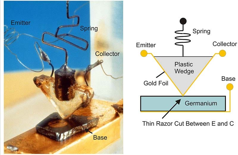
That work inspired Bardeen and Brattain to build a novel device: two gold-foil “cat-whisker” contacts pressed less than a millimeter apart onto an oxidized slab of germanium, with a third contact on the reverse side. When they applied power on December 16, 1947, the current through one whisker controlled the current through the other; the first successful transistor was born.

Bell Labs’ point-contact transistor replaced glass valves with a match-head of germanium. It used one-hundredth the power and survived G-loads that shattered tubes, clearing the first hurdle toward guided munitions3.
Texas Instruments: Integrated Circuit
In the summer of 1958, Texas Instruments engineer Jack Kilby set out to eliminate the maze of wires required to connect separate transistors. His insight was simple: fabricate every component, including transistors, resistors, and capacitors, on a single piece of semiconducting crystal instead of on many individual ones.
While most of the TI staff were on vacation, Kilby built a proof-of-concept on a tiny bar of germanium. The prototype combined one transistor, a capacitor, and three resistors, all linked by short gold “flying-wire” connections etched directly on the same crystal. When he powered it up on 12 September 1958, the circuit oscillated exactly as predicted, proving that an entire electronic function could live on one integrated circuit, or “microchip.”
Because each microchip is literally a small “chip” sawn from a larger semiconductor wafer, Kilby’s invention slashed size and weight, boosted reliability, and launched the era of modern microelectronics.
Monolithic Circuits: Mass Production Unlocked
Early integrated circuits (IC) were hard to scale because microscopic dust particles often contaminated exposed transistor junctions, causing failures. In 1959, Fairchild engineer Jean Hoerni introduced the planar process to address this problem. He coated each silicon wafer with a thin layer of silicon dioxide glass, etched tiny openings where dopants were needed, and left the oxide everywhere else as a sealed barrier. The protective film shielded the devices from airborne impurities and sharply improved manufacturing yield and reliability.
Soon afterward, Robert Noyce, also at Fairchild, realized that the planar process could place many transistors on a single slice of silicon and connect them with aluminum lines laid directly on top of the oxide. His monolithic integrated circuit contained no separate wires; the entire circuit formed one solid block of silicon, which made it smaller, more reliable, and less power-hungry than Jack Kilby’s earlier hybrid device4.
Space Race and Missiles: Fueling the Chip Boom
Sputnik's 1957 beep terrified the U.S., birthing NASA and Kennedy's Moon shot. Apollo's Guidance Computer packed 5,600 NOR gates into flat-pack chips, demanding radiation-hardened reliability. NASA bought 60% of all ICs in 1962-63, funding quality leaps that landed Eagle in 1969, and seeded a $257 billion (inflation-adjusted) semiconductor industry.
Meanwhile, Minuteman II missiles crammed 2,000 chips per guidance unit into a shoebox-sized, enduring launch Gs. The program's demand for 1,000 missiles was so high that it forced the automated production, dropping IC prices tenfold and proving military demand could bankroll civilian tech.
A "Kodak Moment": Photolithography Sparks Moore's Law
One of the major hurdles in miniaturization was that early semiconductor manufacturing was heavily dependent on manual processes for patterning and masking. Workers would physically apply masks and etch patterns onto silicon wafers by hand. This process was labor-intensive and highly prone to human error, resulting in inconsistencies and defects in the final products.
In the 1950s, Jay Lathrop and chemist James Nall at the U.S. Army Diamond Ordnance Fuze Laboratory reasoned that if a microscope could be used to make small images large, then reversing a microscope's optics should result in making large images small. They adapted this approach to project circuit patterns onto germanium using light-sensitive chemicals from Kodak called photoresists, which react when exposed to light, hence coining the term “photolithography” for this semiconductor application. Shining light through a mask with the desired pattern onto a germanium substrate coated with Kodak’s photoresist could create a precise, miniature version of the pattern. Additionally, they realized they could “print” wires by adding an ultra-thin layer of aluminum to connect the germanium components with an external power source. The experiment etched 100-micrometer lines, a joke by today’s standards, but 10× tighter than hand-soldering.
The precision of photolithography made it possible to increase the density of transistors on a single chip dramatically. This enabled the exponential growth in computing power described by Moore’s Law—the observation that the number of transistors on a chip doubles approximately every two years. Without photolithography, the miniaturization and complexity required for modern integrated circuits would not have been achievable, proving that optics, rather than hand-soldering, would set the ultimate size limits.
Photolithography's March: From Crude Lines to Bunker-Busting Brains
Fast-forward to the 1970s: Near-UV light at 365 nm let contact printers crank out 10-micrometer features. Suddenly, you could squeeze a full 16-bit microprocessor into a tiny package—think early Paveway laser-guided bombs, where a single chip called the shots for pinpoint strikes.
By the 1980s and '90s, deep UV step-and-repeat systems with 248 nm and 193 nm excimer lasers dropped lines below 500 nm. We're talking about a 32-bit RISC core, GPS decoder, and high-precision analog-to-digital converter all on one die. That's the secret sauce in Joint Direct Attack Munition (JDAM), turning dumb munitions into GPS-guided nightmares for hardened targets.

The 2000s brought immersion deep ultraviolet lithography (DUV) and multi-patterning, hitting 14 nm nodes. On-chip caches, adaptive seekers, and early tensor processors emerged, perfect for weapons that learn and adapt mid-flight.
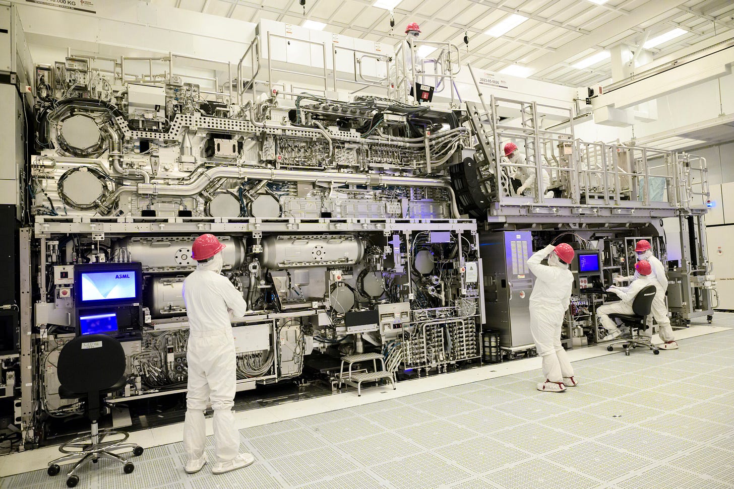
And today? Extreme ultraviolet (EUV) lithography from ASML's beastly $200-million machines blasts 13.5 nm light to carve under 5 nm. Chips like FalconEdge's 3-nm gate-all-around transistors pack more compute than a '90s supercomputer into something poker-chip-sized. For a B-2 stealth bomber eyeing Fordow's underground bunkers, that's the edge: surgical precision that codes its way through concrete, no carpet-bombing required.

MEMS: The Tiny Machines That Made Bombs Shockproof
Chips alone compute; they need senses to navigate chaos. Enter MEMS—Micro-Electro-Mechanical Systems—the 1980s breakthrough blending silicon circuits with microscopic mechanical parts like accelerometers and gyroscopes. Born from DARPA-funded research at places like UC Berkeley and Sandia Labs, MEMS etched tiny beams and rotors into wafers, creating sensors smaller than a grain of sand that detect motion, vibration, and orientation.
This was revolutionary for munitions: Traditional inertial units were fridge-sized and fragile; MEMS shrunk them to chips that survive 10,000g impacts, like slamming into concrete at Mach speeds without flinching. In JDAMs and GBU-57s, MEMS gyros fuse with GPS to correct mid-flight wobbles, enabling that same-hole precision on Fordow. Costs? Plummeted from thousands to dollars per unit, thanks to fabs borrowing photolithography processes.
Today, defense startups are stacking MEMS with AI for autonomous drones and hypersonics—rugged, cheap sensing that's your next deep tech bet.
Meet the GBU-57: The Bunker-Buster Built to Crack Fordow
It's 2009: U.S. intel spots a massive nuclear enrichment buildout in Iran's mountains—Fordow, buried under 80 meters of limestone, cranking out weapons-grade uranium. Problem? No U.S. weapon could punch that deep. Cue the GBU-57 Massive Ordnance Penetrator program, fast-tracked to target such hardened sites.
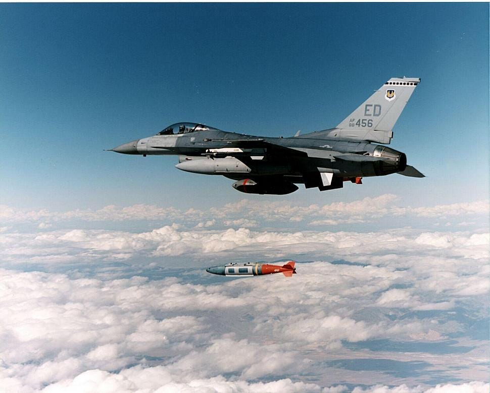
Fifteen years of grind followed: Analysts obsessed over Fordow's layout, geology, and vents, partnering with Boeing and Northrop Grumman to craft a 30,000-pound monster—20.5 feet long, 31.5 inches wide, loaded with 5,300 pounds of AFX-757 explosive. Dropped from a B-2 at 50,000 feet, it hits Mach 1+, guided by grid fins and GPS/INS for meter precision. Its smart fuse "counts" rock layers, detonating inside to shred tunnels.
Testing was hell: Drops at White Sands, rocket sleds, supercomputer sims. Operational by 2011, with 20+ in stock by 2015 and more in 2024. It penetrates 200 feet of concrete, but Fordow's tougher rock needs multiples. Case in point: Operation Midnight Hammer, on June 22, 2025, seven B-2s dropped 12 GBU-57s on vents (six per shaft), blasting through caps and exploding inside. Two more hit Natanz; Tomahawks cleaned up Isfahan. Result? Iran's nuke program stalled for years, per U.S. assessments, though debate lingers on full damage.
Connecting the Dots
Transistor density, driven by Moore's Law, crams inertial, GPS, and AI cores into palm-sized modules for same-hole accuracy. MEMS ensures sensors endure 10,000-g impacts on concrete. Cost drops make six GBU-57s cheaper and cleaner than sixty 2,000-pounders.
Moore's gates provide computing, MEMS adds rugged sensing, and smart-bomb tech from Paveway to JDAM to StormBreaker supplies the AI playbook. EUV lithography keeps it rolling, enabling sub-5nm features for denser, faster chips. Stack 50 years of this, and a B-2 turns penetrators into synced skydivers, dusting Fordow's halls with minimal fallout. For defense startups in AI silicon or sensors, it's your edge: precision over brute force, ripe for investment.
https://www.defense.gov/News/News-Stories/Article/Article/4227082/historically-successful-strike-on-iranian-nuclear-site-was-15-years-in-the-maki/
https://en.wikipedia.org/wiki/William_Shockley
Miller, Chris. 2022. Chip War: The Fight for the World's Most Critical Technology
https://en.wikipedia.org/wiki/Invention_of_the_integrated_circuit


